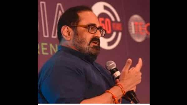
New Delhi: Minister of state for electronics and data know-how, Rajeev Chandrasekhar on Friday inaugurated the Methods and Silicon Innovation lab at NXP Semiconductors Campus in Bengaluru.
The newly inaugurated state-of-the-art lab might be used to design, confirm and validate NXP applied sciences in areas of safety, connectivity, sensing, and processing and construct market-specific system options in automotive, Industrial, IoT, and Shopper areas.
The minister stated, “We wish NXP to proceed with the nice work, working intently with the Startups and accomplice with the native ecosystem to co-create options for the India market.”
Whereas interacting with the NXP-mentored startups, Chandrasekhar stated that they need to proceed to work on strengthening the semiconductor ecosystem in India with a stronger imaginative and prescient and roadmap whereas making good use of presidency incentives and business partnerships.
“The group at NXP India constantly emphasizes creating cutting-edge options which are safe and secure for finish customers. We’re pleased to announce the launch of our new R&D lab that may push innovation within the semiconductor business in India,” stated Hitesh Garg, India Nation Supervisor, NXP Semiconductors.
He added that authorities initiatives like Design Linked Incentive schemes are laying particular emphasis on strengthening the startup ecosystem within the nation. “It’s the want of the hour for international corporates to work on corporate-startup collaborations to provide momentum to newer IP and SoC areas, particular wants of the Indian ecosystem, and system options for ESDM incumbents in India.”
Obtain The Mint News App to get Each day Market Updates & Dwell Business News.
Supply: Live Mint